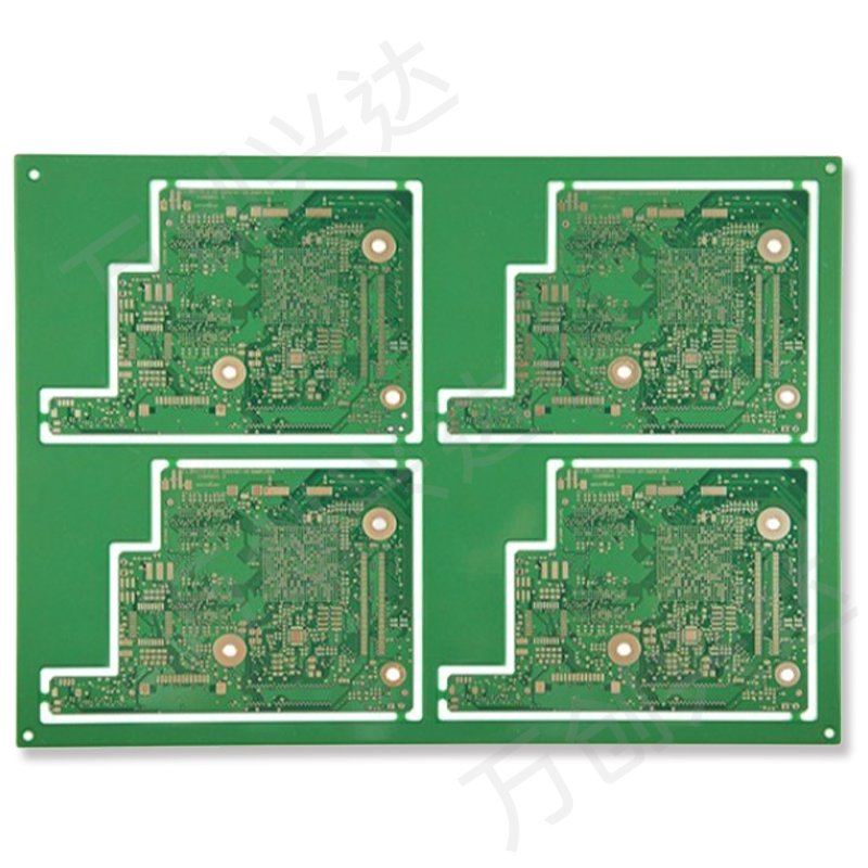
10-layer 1st level FR-4 immersion gold HDI circuit board
Material: Fr-4
Layer Count: 10 layers
PCB Thickness: 1.6mm
Min. Trace / Space Outer: 3/3mil
Min. Drilled Hole: 0.25mm
Via Process: Tenting Vias
Surface Finish: heavy gold
HDI PCB board introduction
HDI circuit board, that is, high-density interconnection PCB board, is a circuit board with relatively high circuit distribution density using micro-blind buried via technology. The HDI board has inner and outer circuits, and processes such as drilling and in-hole metallization are used to connect the circuits in each layer internally.
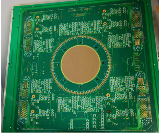
HDI circuit board are generally manufactured using the lamination method. The more laminations, the higher the technical grade of the board. Ordinary HDI circuit boards are basically one-time lamination, while high-end HDI uses two or more lamination technologies, as well as advanced PCB technologies such as stacked holes, electroplated hole filling, and laser direct drilling.
When the density of PCB circuit boards increases beyond eight layers, the cost of manufacturing with HDI will be lower than the traditional complex lamination process. HDI boards are conducive to the use of advanced construction technology, and their electrical performance and signal accuracy are higher than traditional PCB circuit boards. In addition, HDI boards have better improvements in radio frequency interference, electromagnetic wave interference, electrostatic discharge, heat conduction, etc.
Electronic products continue to develop toward high density and high precision. In addition to improving machine performance, the size of the machine must also be reduced. High-density integration (HDI) technology enables end product designs to be more miniaturized while meeting higher standards of electronic performance and efficiency. Many of the currently popular electronic products, such as mobile phones, digital cameras, laptops, automotive electronics, etc., use HDI boards. With the upgrading of electronic products and market demand, the development of HDI boards will be very rapid.
HDI circuit board production process
The high density of HDI boards is mainly reflected in the density of holes, lines, pads, and interlayer thickness.
● Micro-guide holes: The HDxI board contains micro-guide hole designs such as blind holes, which are mainly reflected in the micro-hole hole forming technology with a diameter of less than 150um and the high requirements in terms of cost, production efficiency and hole position accuracy control. There are only through holes in traditional multi-layer circuit boards and there are no tiny buried blind holes.
● Refinement of line width and line spacing: This is mainly reflected in the increasingly stringent requirements for wire defects and wire surface roughness. Generally, line width and line spacing do not exceed 76.2um
● High pad density: welding contact density is greater than 50 per square centimeter
● Thinning of dielectric thickness: This is mainly reflected in the trend of inter-layer dielectric thickness to 80um and below, and the requirements for thickness uniformity are becoming more and more stringent, especially for high-density boards and packaging substrates with characteristic impedance control

How to distinguish between first-order, second-order and third-order HDI PCB
● After pressing once, drill holes==> Press the copper foil again on the outside==> Then laser drill holes, this is the first stage,The first level is relatively simple, and the process and technology are easy to control.
● Laminate the copper foil once==>Lay the outer layer of copper foil again==>Laser again,==>Lay the outer layer of copper foil again==>Laser again. This is level two. The main thing is to see how many times you use laser, which is the level.,The second level starts to have troubles, one is the alignment problem, and the other is the drilling and copper plating problem. There are many second-stage designs. One is to stagger the positions of each stage. When the next adjacent layer needs to be connected, it is connected through wires in the middle layer. This is equivalent to two first-order HDIs. The other is that two first-order holes overlap, and the second-order is realized through superposition. The processing is similar to two first-order holes, but there are many process points that need to be specially controlled, which are mentioned above.
● For the third order, the second order is analogous.
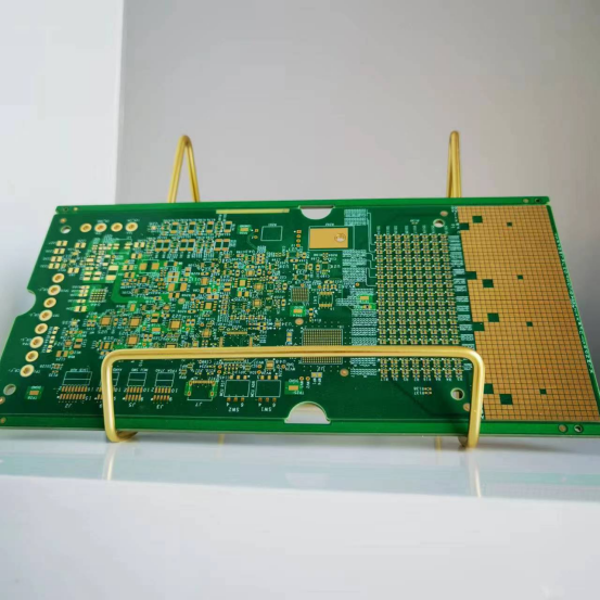
HDI circuit boards have very high requirements for buried hole plug holes
Whether it is the size of the board or the electrical performance, HDI is superior to ordinary PCB. The other side of HDI is that as a high-end PCB, its manufacturing threshold and process difficulty are much higher than that of ordinary PCB, and there are many issues that need to be paid attention to during production – especially buried hole plug holes. At present, the core pain point and difficulty in HDI production and manufacturing is buried hole plugging. If the HDI buried hole is not plugged properly, major quality problems will occur, including uneven board edges, uneven media thickness, and pitted pads.

